In 2025, career options in PCB include medicine, biotechnology, environmental science, pharmacy, and research, reflecting different interests and attracting different students.
Some students may want to work as a doctor, a biochemist, a nutritionist, or an ecologist as there will be a high demand for all those professions especially in the health and life sciences.
In general, post graduate studies, certifications, and hands-on training, can increase any student’s job prospects and earnings.
Table of Contents
Wondering what are the best careers one can take after choosing PCB (Physics, Chemistry, Biology) in your 12th grade? 2025 presents an opportunity for a PCB student to be in the crème de la crème for job and career opportunities in some of India’s most skilled and high-growth professions. PCB career opportunities are broader and better than before and encompass traditional careers in medicine and pharmacy and modern careers in biotechnology, environmental science, and research.
This article serves as a guide for students interested in PCB careers and will explain the suitability of careers with PCB educational requirements, skills, and future career opportunities. Whether you are more interested in life sciences, healthcare, or technology, this article provides useful tips and the latest trends aligned with PCB job and industry requirements and examples of career paths. Explore possibilities for your career and prepare for a fulfilling career with a PCB background.
What Are PCB Career Options?
PCB stands for Physics, Chemistry, and Biology, which are subjects chosen by students in their 11th and 12th grades. These subjects open doors to a wide range of career opportunities in fields like medicine, research, engineering, and more. The phrase pcb career options refers to all the professional paths you can take after completing your studies with these subjects.
For Indian students, PCB is often seen as the gateway to becoming a doctor. However, it’s important to know that there are many other exciting and rewarding careers beyond MBBS. Let’s dive into some of the most popular and promising pcb career options in India.
How to Choose the Right Course After the 12th PCB?
Prior to deciding on a PCB career idea, detrime whether to weigh:
Interest in Fields
Medical (MBBS, Nursing, Physiotherapy)
Research and Biotechnology (Biotech, Genetics, Laboratory Research)
Technology and Engineering (Biomedical Engineering, Data Science in Biology)
NEET vs Non-NEET Options
NEET-required courses: MBBS, BDS, AYUSH
Non-NEET options: BSc, Biotechnology, Microbiology, Pharmacy, Research programs
Long-term Goals, Occupational and Growth Potential
Job stability, scope for career progression or higher studies
Possibility for research/innovation in the chosen field
Finances
Modification of tuition fees, scholarship opportunities, stamp of return of investment (ROI) on your field
Cost compared to earnings and satisfaction attracts through a career change in the long term.
Backup Career Options
Alternative career paths just in case your first idea fails or doesn’t work out
Related areas utilizing the same PCB education (e.g., lab technician, teaching, science communication)
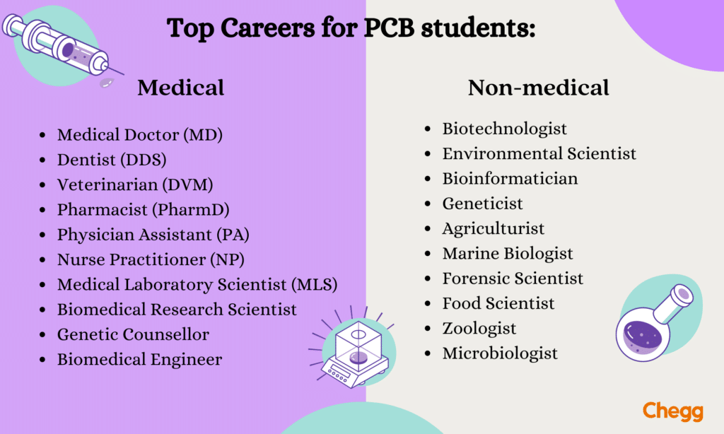
Top PCB Career Options (Medical)
Here is a list of popular after 12 PCB career options in the medical field:
1. Medical Doctor (MBBS)
a) Job Description
Identify, treat, and prevent illnesses and injuries.
Recommend medications and treatment plans.
Monitor progress and provide long-term care for patients.
Educate and supervise junior doctors and interns.
b) Qualification:
10+2 with a major in PCB (minimum aggregate 50% marks).
Qualification in NEET-UG for admission.
Course Duration and Pathway: MBBS (5.5 years including internship) – MD/MS Specialization (3 years).
c) Salary Progression Table:
Level
Experience
Average Monthly Salary (INR)
Entry (Resident Doctor)
0–2 years
1,00,000 – 2,00,000
Mid-Level (Consultant)
3–8 years
2,50,000 – 5,00,000
Senior (Specialist / Surgeon)
10+ years
6,00,000+
d) Future Demands & Industry Opportunities:
Increase in demand for specialists in oncology, neurology, and telemedicine.
Increase in demand for Indian doctors overseas – Gulf and Europe.
e) Example in Industry:
Dr. Riya Sharma, MBBS (AIIMS), trained as a Resident at ₹1.2L/month, would earn up to ₹5L/month if promoted to a Consulting Cardiologist after 7 years.
A Dentist (DDS), or Doctor of Dental Surgery, is a medical professional specializing in the care, prevention, and treatment of oral and dental health issues.
a) Job Description
Diagnosing and treating patients for problems relating to the mouth and teeth.
Extract teeth, carry out fillings, complete root canals, do prosthesis fittings.
Suggest preventive care for patients.
b) Qualifications
10+2 in PCB.
Must qualify NEET-UG.
BDS (5 years with internship) -> MDS (3 years.)
c) Salary Progression Table
Level
Experience
Average Annual Salary (INR)
Entry
0–2 years
4–6 LPA
Mid-Level
3–7 years
8–12 LPA
Senior
8+ years
15–25 LPA
d) Future Trend / Scope
Growth in cosmetic dentistry and dental tourism in India.
Increase in employment opportunities in private practice – clinics and hospitals.
e) Example in Industry:
Dr. Nikhil Verma completed his MDS in Orthodontics and has his own clinic in Pune, earning ₹20L annually.
3. Veterinarian (DVM)
Popularly called a Vet, a Veterinary Doctor treats animals and birds for different ailments. You can pursue a Diploma or UG course in Veterinary Medicine after school.
a) Job Description
Diagnose and treat injuries and diseases in animals.
Perform surgeries and vaccination clinics.
Educate pet parents on animal health, nutrition, and hygiene.
b) Qualifications
10+2 with a PCB focus.
Entrance Test: NEET-UG / State Veterinary CETs.
Time to complete pathway: BVSc (5.5 years) → MVSc (2 years).
c) Salary Progression Table
Level
Experience
Average Annual Salary (INR)
Entry
0–3 years
6–8 LPA
Mid-Level
4–8 years
9–14 LPA
Senior
10+ years
18–25 LPA
d) Future Scope and Trends:
Increased demand for pet healthcare and livestock care.
Increasing demand for animal biotechnology and wildlife conservation.
e) Example in Industry:
Dr. Sneha Iyer started as a Govt. Vet Officer at ₹7.5 LPA, and now she runs a private animal hospital in Bangalore.
A Pharmacist (PharmD) is a healthcare professional who specializes in the preparation, dispensing, and proper use of medications.
a) Job Description
Safely dispense prescribed medication.
Verify dosage and provide advice on medication administration.
Interact with physicians for therapeutic assessment.
b) Qualifications
Class 12 with PCB major.
Entrance: GPAT, MHT-CET, BVP CET, MET.
Duration and Pathway: Bachelor of Pharmacy (4 Years), Master of Pharmacy (2-6 Years).
c) Salary Progression Table
Level
Experience
Average Annual Salary (INR)
Entry
0–2 years
3–5 LPA
Mid-Level
3–7 years
6–9 LPA
Senior
8+ years
10–15 LPA
d) Future Scope and Trends:
Increase in clinical research, pharmaceutical analytics, and drug manufacturing.
More and more global opportunities in pharmacovigilance.
e) Example in Industry:
Ravi Menon, Pharm. D. started as a community pharmacist with a salary of 4,00,000 per annum, and subsequently worked as a Pharmaceutical Quality Assurance Analyst for 12,00,000 per annum.
5. Physician Assistant (PA)
A Physician Assistant (PA) is a highly trained healthcare professional who works under the supervision of a licensed physician to provide medical care.
a) Job Description:
Collaborate with physicians to assess, diagnose, and care for patients.
Carry out minor procedures and handle emergencies.
b) Qualifications
10+2 with PCB major.
Entrance: CUET, State CETs, or institutional entrance exams.
Duration and path: B.Sc. (3 years) → M.Sc. (2 years).
c) Salary Progression Table
Level
Experience
Average Annual Salary (INR)
Entry
0–2 years
5–6 LPA
Mid-Level
3–6 years
7–10 LPA
Senior
8+ years
12–14 LPA
d) Future Scope & Trends:
Increased usage in telehealth and surgical support teams.
Increased hiring in Tier-2 hospitals and private practices.
6. Nurse Practitioner (NP)
AN NP is a health professional offering patients acute, primary, and emergency care. To become an NP, you must have aBachelor’s Degree in Nursing (BSc).
a) Job Description:
Global immigration is possible for nurses searching for work based on nursing and health skills developed in Canada.m INR 2,50,000 to 3,00,000 per annum.
Delivering patient-centered care by assessing, diagnosing, and managing their cases.
Formulating and implementing community health programs, including conducting clinical research.
b) Qualifications:
Candidates must have earned their higher secondary qualification from a recognized institute with PCB as their primary subject.
Admission based on entrance examination results: AIIMS B.Sc. Nursing, NEET, State Nursing CETs.
Expansion of diagnostics chains, hospital labs, and biotech testing labs.
Automation of processes in the lab is increasing productivity and demand.
8. Biomedical Research Scientist
A Biomedical Research Scientist conducts laboratory research and scientific tests to help diagnose and treat diseases. It is one of the best PCB Career Options after the 12th.
a) Job Description:
Develop and execute experimental research to contribute to medical research.
Expansion in genomics, immunology, and AI-based diagnostics.
High international demand for R&D and pharma.
9. Genetic Counselor
Genetic counselors work directly with patients to determine the risks and advantages of their genetics. For example, they assess the risks of genetic diseases with couples wanting to have a child.
a) Job Description:
Consult/perceive patients regarding hereditary and genetic maladies.
Facilitate genetic testing and interpret the results.
Trends towards genomic medicine and prenatal testing.
Extreme efficacy with the current move towards personalized healthcare.
10. Biomedical Engineer
A Biomedical Engineer develops medical products, software, and computer systems to find a solution to healthcare problems.
a) Job Description:
Create medical devices, prosthetics, and diagnostic systems.
Work collaboratively with hospitals and R&D teams.
b) Qualifications:
10+2 with PCB is a prerequisite.
Entrance: JEE, State CETs, or CUET.
Program Duration and pathway: B.Tech (4 years) → M.Tech (2 years)
c) Salary Progression Table:
Level
Experience
Average Annual Salary (INR)
Entry
0–2 years
3–5 LPA
Mid-Level
3–7 years
6–10 LPA
Senior
8+ years
12–18 LPA
d) Future Scope & Trends:
Growth in robotic medicine, wearables, and artificial intelligence in healthcare.
Collaboration possibilities with global medical technology companies.
Top PCB Career Options (Non-Medical)
There are ample PCB career options not just in the medical field but also in non-medical streams. Popular PCB courses for students with non-medical career options are listed here.
11. Biotechnologist
A biotechnologist develops new technologies by combining Biology and Technology. They study and manipulate a cell’s chemical, physical, and genetic attributes to address issues like vaccines, medicines, energy efficiency, food shortages, etc.
a) Job Description:
Creating, conducting, and monitoring experiments on live organisms.
Perform data analysis using scientific methodologies to interpret findings.
Record and document findings for publications.
Develop new products, processes, and techniques.
b) Qualifications Required:
10+2 with a PCB major
Clear entrance exams like JEE, WBJEE, BHU UET, JMI EE, UPCET, etc.
UG Courses: B.Sc. in Biotechnology or B.Tech. / BE in Biotechnology
PG Courses: M.Sc. / M.Tech. / ME in Biotechnology
c) Average Salary:
The average Junior Biotechnologist’s salary is approximately INR 4,96,000 per annum.
12. Environmental Scientist
You will study the impact of natural and artificial phenomena on the environment. This field focuses on ecology, geology, meteorology, biology, chemistry, engineering, and physics. It is an essential field that shapes international environmental policies.
a) Job Description:
Plan for prevention and fixing of environmental issues.
Collect and analyze geological, geochemical, and geophysical information.
Interpret the data to provide solutions for environmental issues.
Investigate soils, minerals, fossil remains, etc.
Assess groundwater movement.
Offer advice regarding waste management, site selection, restoring contaminated sites, etc.
Locate and estimate natural resources such as oil, minerals, etc.
Identify and warn about natural adversaries such as earthquakes, volcanic eruptions, etc.
b) Qualifications Required:
10+2 with a PCB major
UG courses: B.Sc. in Environmental Science or B.Tech. in Environmental Science.
PG courses: M.Sc. in Environmental Science or M.Tech. in Environmental Science.
c) The average salary:
For a fresher is approximately INR 6,16,000 per annum.
13. Bioinformatician
This is one of the best career choices for people who love Biology and Information Technology. Complex biological data can be analyzed faster with computational capabilities. The process is accurate and time-saving.
a) Job Description:
Develop codes to analyze biological samples and databases.
Develop software for data studies and comparisons.
Design tools for data modeling, visualization, exploring, and interpreting.
Provide global biological databases that scientists can access to search and analyze information.
Develop new tools as per project and research requirements.
b) Qualifications Required:
10+2 with a PCB major
UG Courses: B.Sc. or B.Tech. in Bioinformatics
PG Courses: M.Sc., PG Diploma or M.Tech in Bioinformatics
c) Average Salary:
The average salaray for a fresher is more than INR 3,42,000 per annum.
14. Geneticist
This is a great PCB career option if you are interested in studying qualities and heredity passed down through the ages. Geneticists study all living organisms, from plants, animals, and humans, to microbes.
a) Job Description:
Collecting DNA samples.
Conducting lab research on collected samples.
Analyzing and interpreting genetic lab results.
Documenting the evaluation results.
Dissecting the information load to arrive at concrete conclusions.
These results will be published in publications, conferences, and research papers.
b) Qualifications Required:
10+2 with a PCB major
Clear JEE Main or CUET
UG Courses: B.Sc. or B.Tech. in Genetics Engineering, B.Sc. Biology, etc.
PG Courses: M.Sc. or M.Tech. in Genetics Engineering, M.Sc. Biology, etc.
c) Average Salary:
The average pay for a fresher is more than INR 11,73,134 per annum.
15. Agriculturist
This is the best career option if you are passionate about agriculture and want to improve the field through scientific methods. The primary objective is to develop the best methods for cultivating soil, livestock rearing, and crop growth.
a) Job Description:
Designing the best pieces of equipment for harvesting while reducing crop damage.
Expertise in crop management, ecosystems, weed and pest control, etc.
Increasing productivity and profitability of livestock farmers.
Focus on animal breeding, living conditions, emergency, disease control, etc.
Genetically modifying crops to make them resistant to certain adverse conditions.
b) Qualifications Required:
10+2 with a PCB major
Diploma Courses: Agriculture, Agriculture and Allied Practices, Food Processing, etc.
UG Courses: B.Sc. in Agriculture, B.Sc. in Crop Physiology, B.Tech. in Agriculture.
PG Courses: M.Sc. in Agriculture, M.Sc. in Biological Studies, M.Sc. in Agriculture Botany, etc.
c) Average Salary:
The average pay for a fresher is more than INR 5,42,000 per annum.
16. Marine Biologist
If you are excited by the oceanic world, this is one of your best career choices. Marine Biologists research and understand aquatic life and ecosystems.
a) Job Description:
Study marine life, including underwater plants, animals, fish, whales, and dolphins.
Gather samples from oceanic floors to learn about species distribution, diseases, etc.
Study the behavior of marine life and its effects on the ecosystem.
Determine the level of pollution and formulate methods to reduce it.
Discover new species of plants, animals, and microorganisms.
Document their discovery and publish research papers.
Educate people about marine life preservation.
Treat marine animals for diseases and reduce invasive species in the area.
b) Qualifications Required:
10+2 with a PCB major
UG Courses: B.Sc. in Marine Biology, Oceanography, Marine Sciences, Earth Sciences, etc.
PG Courses: M.Sc. in Marine Biology
c) Average Salary:
The average pay for a fresher ranges from INR 8,45,140 to 14,64,829 per annum.
17. Forensic Scientist
Do crime laboratories enthrall you? You must choose to become a Forensic Scientist. The Forensic scientist analyses evidence from the crime scene and provides opinions based on chemical and physical examinations.
a) Job Description:
Examine evidence from the crime scene.
Conduct investigative physical and chemical analyses of the evidence.
Generate reports based on the findings in a written document.
Coordinate with other departments, such as Police or CBI.
Mentor forensic scientist interns.
b) Qualifications Required:
10+2 with a PCB major
UG Courses: B.Sc. in Forensic Science, Biology, Forensic Anthropology or Genetics; B.Tech. in Genetic Engineering, Biotechnology, Computer Science in Cybersecurity and Forensics, Information Security, etc.
PG Courses: M.Sc. in Forensics, Chemistry, Biology, Toxicology, etc. M.Tech. in Biotechnology, Genetic Engineering, Information Security and Digital Forensics, etc.
c) Average Salary:
The average salary for a fresher ranges from INR 7,96,477 to 13,67,324 per annum.
18. Food Scientist
Are you interested in the science behind food production, processing, and preservation? You should consider becoming a Food Scientist, as it is one of the best PCB career options after 12th. It involves science in food preparation, processing, packaging, and preservation.
a) Job Description:
Evaluating the nutritional value, flavor, and texture of food.
Designing and producing equipment to produce and package food on a large scale.
Testing food samples.
Ensuring adherence to government norms.
Exploring optimal alternative methods at low cost.
Inspecting for safety and quality.
b) Qualifications Required:
10+2 with a PCB major
UG Courses: B.Sc. in Food Science, B.Tech. in Food Technology
PG Courses: M.Sc. in Food Science, M.Tech. in Food Technology
c) Average Salary:
The average pay for a fresher is approximately INR 5,13,000 per annum.
19. Zoologist
If you are interested in animals and their evolution, you must consider becoming a zoologist. It is one of the best career options for PCB students with various industries to work for as a zoologist.
a) Job Description:
Conduct experiments on animals in a controlled or natural setting.
Research and analyze behaviors such as reproduction, population, illnesses, etc.
Study the impact of human actions on wildlife.
Improve breeding and preserve endangered animals.
Monitor and explore invasive species.
b) Qualifications Required:
10+2 with a PCB major
UG Courses: B.Sc. in Zoology, Animal Ecology, Animal Science, etc.
PG Courses: M.Sc. in Zoology, Animal Ecology, Animal Science, etc.
c) Average Salary:
The average pay is approximately INR 11,70,257 per annum.
20. Microbiologist
Microbiologists study microscopic organisms and their interactions with humans and other organisms. They are employed in various industries, such as food, green technologies, and climate studies.
a) Job Description:
Plan and carry out research projects.
Perform lab experiments for disease diagnosis and treatment.
Isolate and keep cultures of microorganisms.
Identify and classify microorganisms.
Make recommendations based on research findings.
b) Qualifications Required:
10+2 with a PCB major
UG Courses: B.Sc. in Botany, Microbiology, Biology, Zoology, etc.
PG Courses: M.Sc. in Microbiology, Biology, Zoology, Botany, etc.
c) Average Salary:
The average pay for a fresher is INR 8,38,000 per annum
High Paying Jobs for PCB Students
Here are some of the most sought-after career options for PCB students with high salary potential after 12th PCB, offering excellent growth prospects:
Medicine and Surgery (MBBS) Become a doctor and later specialize in fields such as cardiology, neurology, or general surgery. This path offers the highest earning potential with experience and specialization.
Dentistry (BDS/MDS) Pursue a career as a dentist. Specializations like orthodontics or oral surgery can lead to outstanding financial rewards along with a fulfilling practice.
Biotechnology Merge biology with technology by exploring careers in genetic engineering, pharmaceutical research, or bioinformatics. This innovative field offers great salaries and research opportunities.
Pharmacy (PharmD) Work as a pharmacist in hospitals, retail settings, or pharmaceutical companies. This option provides a stable and financially rewarding career as healthcare technology evolves.
Nutrition and Dietetics Specialize in nutrition, working as a consultant or within hospitals and wellness centers—demand is growing for experts in healthy lifestyle and diet management.
AYUSH Careers Explore traditional medicine streams like Ayurveda, Yoga, and Homeopathy. With increasing integration of holistic health practices, specialists in these fields can secure solid incomes.
Physiotherapy Focus on physical therapy and rehabilitation. With rising demand in sports medicine and patient care, specialized physiotherapists are well compensated.
Medical Laboratory Technology Step into the role of a diagnostic expert. Working in clinical laboratories, this career involves analyzing tests and ensuring accurate diagnoses—all within a growing, high-demand segment of healthcare.
Each of these PCB student career options is designed to align with your interests and strengths as a PCB student, combining personal fulfillment with impressive salary prospects.
Top Courses after 12th PCB: Eligibility, Admission, Salary
Here is the after 12th PCB courses list in a structured table format:
Entrance tests, Direct admission in some universities
Drug Therapist, Hospital Pharmacy, Researcher
₹10,000 – ₹18,000 per month
BPT
10+2 with minimum 50% marks in PCB + English
4 years
Entrance exam
Sports Physio, Research Assistant, Lecturer
₹15,000 – ₹30,000 per month
BUMS
10+2 with minimum 50% marks in PCB
5.5 years
NEET
Private Practice, Public Health Specialist
₹12,000 – ₹15,000 per month
Microbiology
10+2 with minimum 55% marks in Science
3 years
Direct/Entrance exam
Microbiologist, Medical Technologist, Researcher
₹10,000 – ₹20,000 per month
Biotechnology
10+2 with minimum 55% marks in PCB or PCM
3-4 years
Entrance test
Biomedical Engineer, Medical Scientist
₹25,000 – ₹28,000 per month
Bioinformatics
10+2 with minimum 50% marks in PCB
3 years
Entrance test + Interview
Clinical Pharmacologist, Informatics Developer
₹2 lakh – ₹3 lakh PA
Forensic Sciences
10+2 with Science
3 years
Entrance test
Crime Scene Investigator, Forensic Medical Examiner
₹3 lakh – ₹4 lakh PA
Genetics
10+2 with Science
3 years
Direct/Entrance exam
Geneticist, Epidemiologist
₹3.5 lakh – ₹5 lakh PA
Nursing
10+2 with PCB as compulsory subjects
4 years
Entrance exams
Nurses, Midwives, Nursing Superintendent
₹2 lakh – ₹2.8 lakh PA
Environmental Science
10+2
3 years
Direct/Entrance exams
Conservation Hydrologist, Director of Waste Management
₹3 lakh – ₹5 lakh PA
Arts and Humanities
10+2 with minimum 50% marks
3 years
Entrance exams
Journalist, Copywriter, Social Worker
₹15,000 – ₹20,000 per month
How to Choose High-Salary Courses after 12th PCB?
Choosing high-salary courses after 12th PCB starts with knowing your interests, researching market trends, and finding the right course that matches both your passion and career goals. Here’s how to decide:
Assess Your Interests: Consider whether you are more inclined toward clinical practice, research, or innovative fields like biotechnology. Knowing your strengths and passion helps narrow down choices.
Research Career Prospects: Look into courses that lead to lucrative roles. Common high-paying options for PCB students include MBBS, BDS, PharmD, Biotechnology, Nutrition & Dietetics, and specialized fields like Radiography or Physiotherapy. Research their average starting salaries, growth potential, and industry demand.
Evaluate Course Content and Specializations: Examine the curriculum and the scope for specialization in each course. For instance, an MBBS degree offers specialization in fields such as cardiology or neurology, which typically have higher earning potential.
Check Accreditation and Institutional Reputation: Enroll in reputed institutions with strong clinical exposure, quality mentorship, and good placement records. Accredited programs enhance your prospects in the competitive job market.
Seek Guidance: Connect with teachers, career counselors, or professionals in the field. Their insights on course quality, future prospects, and real-world challenges can guide you in making an informed decision.
Consider Long-Term Growth: Think beyond your first job. Choose courses that offer pathways for advanced studies, research, or specialization. A strong foundation now can open doors for lucrative, long-term career growth.
By following these steps and doing thorough research, you can select a robust, high-salary courses for PCB students after 12th that sets you on a rewarding career path after 12th PCB.
Choose the Best PCB Career Path for You
Numerous PCB career options, both medical and non-medical, are outlined here, providing students with valuable insight for informed decision-making. Your ideal career path depends on your unique skills and interests. Review the details provided for each option and select the one that resonates with you. Making the right choice can significantly impact your career success, so ensure it aligns with your passions. Explore various career options to find the perfect fit for you. Explore a wide range of PCB career options without NEET, including fields like biotechnology, pharmacy, environmental science, and clinical research, offering promising career opportunities without the need for a medical entrance exam. For more guidance, delve into our comprehensive Career Advice guide.
Tips for Choosing the Right Career Options After 12th PCB
Here are some tips for choosing career options after 12th Science PCB (Physics, Chemistry, and Biology):
Assess interests and strengths: Reflect on enjoyable subjects and performance in fields that align with aptitudes.
Research various career paths: Explore options like medicine, dentistry, veterinary science, biotechnology, environmental science, and allied health.
Consider long-term goals: Consider where you see yourself in 5-10 years.
Evaluate academic performance: Be realistic about grades and exam scores.
Explore emerging fields: Explore genetic engineering, bioinformatics, or forensic science.
Consult with professionals: Gain a realistic view of the profession.
Consider financial aspects: Research costs of further education and potential starting salaries.
Attend career fairs and counseling sessions: Gain valuable information.
Look into interdisciplinary options: Consider fields like biomedical engineering or health management.
Keep alternative options open: Have backup plans in case of a primary choice.
Conclusion
As you consider career paths within the PCB umbrella, you’ll discover a fascinating and fulfilling array of possibilities open to students interested in science and health to engage in meaningful work. Whether you’d like to become a physician, researcher, biotechnologist, or environmental health specialist, you can be sure that a strong foundation in PCB opens viable and respected professional pathways for the future.
Remember, ultimately, the best career path will be a combination of your interests, strengths, and goals for the future. In the meantime, remember to stay inquisitive and vigilant about changes within your ecosystem. Seek mentorship from subject matter experts, your instructors, or career services. If you are open to and seek out new opportunities and fields of study, and with preparation, you will be well-equipped to explore and build a career in the changing landscape of science or healthcare.
Frequently Asked Questions (FAQ’s)
What is the best career in PCB?
The best career in PCB depends on your interests. Popular options include medicine (MBBS), dentistry (BDS), biotechnology, environmental science, and paramedical fields like physiotherapy and nursing. These careers offer growth and stability.
Which is the best job without NEET?
High-paying jobs without NEET include biotechnology, pharmacy, clinical research, psychology, and food technology careers. These fields offer excellent opportunities without requiring NEET qualification.
Is PCB good for future?
Yes, PCB offers excellent career opportunities in medicine, biotechnology, forensics, and environmental science. Even without NEET, high-paying options like biomedical engineering, psychology, and nutrition are available.
Which is the highest-paying jobs in PCB?
The highest-paying jobs in PCB are typically in medicine, such as surgeons, neurologists, and cardiologists. Other lucrative fields include biotechnology, forensic science, and environmental science.
Is PCB or PCM better?
PCB is best for medical careers like doctor, pharmacist, or biotechnologist, while PCM is ideal for engineering, architecture, and tech fields. Choose based on your interests!
Which course after 12th PCB has the highest salary?
Courses like MBBS, BDS, B.Sc in Biotechnology, and B.Pharm lead to high-paying careers. Specializations in biotechnology or environmental science also offer competitive salaries.
Example: For example, MBBS, BDS, or B.Sc in Biotechnology are considered high salary courses after 12th science biology with strong future prospects. Tip: Choose pcb courses after 12th based on market demand, specialization potential, and your personal interests.
What to do after 12th PCB without NEET?
After completing 12th with Physics, Chemistry, and Biology (PCB) without aiming for NEET, you can explore various fields like nursing, pharmacy, biotechnology, microbiology, or pursue a Bachelor of Science in areas like nutrition, agriculture, or forensic science.
Example: For instance, pursuing B.Sc in Nutrition or Clinical Research are great pcb career options without NEET offering strong placement opportunities. Tip: Always explore courses for PCB students after 12th that align with your strengths and offer long-term growth.
Which doctor has the highest salary?
In the field of medicine, Neurosurgeons generally earn the highest salaries
Which career is best after PCB?
There are several promising career options after 12th Science PCB without NEET, including Veterinary Science, Pharmacy, Psychology, Food Engineering, Nursing, Optometry, Physiotherapy, and Agriculture. These after 12th PCB courses offer great scope, making them ideal career options for PCB students seeking stability, growth, and high-salary opportunities beyond traditional medicine.
Authored by, Gagandeep Khokhar Career Guidance Expert
Gagandeep is a content writer and strategist focused on creating high-performing, SEO-driven content that bridges the gap between learners and institutions. He crafts compelling narratives across blogs, landing pages, and email campaigns to drive engagement and build trust.